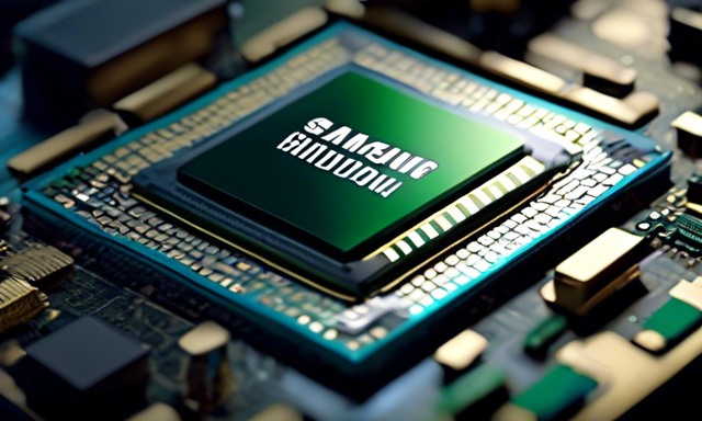
Breaking News: Samsung’s HBM3E Chips Pass Nvidia’s Tests for AI Processors!
A new milestone has been achieved in the world of technology as Samsung’s fifth-generation HBM chips, known as HBM3E, have successfully passed Nvidia’s tests for use in their AI processors. This development comes as a significant breakthrough for Samsung, positioning them as a key player in the competitive market of advanced memory chips designed to support generative AI work. Here’s what you need to know about this groundbreaking achievement:
The Approval Process
Here are some key points to consider regarding Samsung’s HBM3E chips and their recent approval by Nvidia:
- Nvidia’s tests have confirmed the viability of Samsung’s HBM3E chips for integration into AI processors.
- The approval signifies a major stride for Samsung in catching up with rivals like SK Hynix in supplying cutting-edge memory solutions for AI applications.
Supply Deal and Timeline
While Samsung and Nvidia are yet to finalize a supply agreement for the approved HBM3E chips, sources indicate that a deal is imminent. Expectations are high that the supply of these chips will commence by the fourth quarter of this year. Here’s what you need to know:
- The agreement for the eight-layer HBM3E chips is expected to be formalized soon.
- Sources anticipate that shipments of the approved chips will begin by the end of 2024.
Future Prospects and Market Impact
Looking ahead, the successful qualification of Samsung’s HBM3E chips opens up a realm of possibilities for the tech giant. Here’s a glimpse into the future implications of this groundbreaking development:
- The 12-layer version of Samsung’s HBM3E chips is still undergoing testing and evaluation by Nvidia.
- Both Samsung and Nvidia have refrained from providing official comments on the matter.
Understanding HBM Technology
To comprehend the significance of Samsung’s HBM3E chips, it’s essential to grasp the fundamental concepts behind HBM technology. Here’s a brief overview:
- HBM (High Bandwidth Memory) is a specialized type of DRAM that involves vertically stacking memory chips to enhance efficiency.
- Integral to GPUs for AI, HBM technology facilitates the processing of vast amounts of data generated by complex applications.
Market Outlook and Growth Projections
The burgeoning demand for advanced memory solutions has set the stage for robust growth in the HBM market segment. Here’s a glimpse into future trends and predictions:
- HBM3E chips are poised to dominate the market in the upcoming months, with a surge in shipments expected in the latter half of this year.
- Research indicates a projected annual growth rate of 82% for HBM memory chips through 2027, fueled by escalating demand for cutting-edge AI technologies.
Key Players in the Industry
As the demand for HBM chips intensifies, major players in the industry are gearing up to meet market demands. Here’s a look at the key manufacturers:
- SK Hynix, Micron, and Samsung are the prominent manufacturers of HBM chips in the market.
- SK Hynix has been a primary supplier of HBM chips to Nvidia, highlighting their pivotal role in the industry.
Hot Take: The Future of AI Processing with Samsung’s HBM3E Chips
In conclusion, the successful testing of Samsung’s HBM3E chips by Nvidia marks a significant milestone in the realm of AI processors. As Samsung solidifies its position as a key player in the advanced memory chip market, the tech industry braces for a new era of innovation and efficiency powered by cutting-edge technologies!


 By
By
 By
By
 By
By

